


WARDE TECHNOLOGY SINGAPORE PTE LTD
was incorporated in July 2012 with a vision to support our regional customers in the Semiconductor and TFT and Solar industries.
About Us

WARDE TECHNOLOGY had already established themselves in the Taiwan and China Semiconductor market since 2003; supporting various major players such as TSMC, UMC, MICRON, SMIC....
read moreOur Services
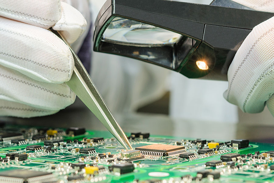
We are also experience in equipment components improvement and modification; overhaul and refurbishment of mechanical and electrical parts such as Motors, Mechanical Actuators and Spindle, Driver Controllers and others parts. We had successful stories in modification of equipment parts and also high success rates for other overhaul and refurbishment projects for customers in the Semiconductor, TFT and Solar Industries.
read more
Our Products Range
We have a wide range of manufacturing and analytical equipment to manufacture a wide range of products and repair capabilities for Semiconductor, TFT and Solar industries.
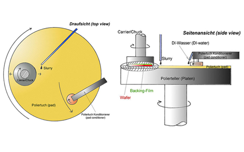
CMP
Chemical Mechanical Planarization (CMP) a polishing process, which utilizes a chemical slurry formulation and mechanical polishing process to remove unwanted conductive or read more
THIN FILM
Thin Film Deposition is the technology of applying a very thin film of material – between a few nanometers to about 100 micrometers, or the thickness of a few atoms – onto a
read more

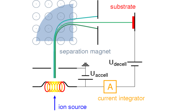
IMPLANT
Ion implantation is low-temperature process by which ions of one element are accelerated into a solid target, thereby changing the physical, chemical, or electrical properties of the
read more

ETCH
Etching is used in microfabrication to chemically remove layers from the surface of a wafer during manufacturing. Etching is a critically important process module, and every read more
Our Services
WARDE TECHNOLOGY provide repair and overhaul of RF components, parts cleaning servicing and material analysis for Semiconductor, TFT and Solar industries. These services are also spread across various Semiconductor process such as CMP, Thin Film, Implant, Etch and others.
- Refurbishment and Overhaul of Mechanical and Electrical equipment and components
- Reverse Engineering of equipment components
- Parts and Component Manufacturing
- Failure Analysis
- Cleaning and Refurbishment services